VLSI
40 Days Intensive Internship

MasterVLSI Design
& Chip Verification

Dive into the world of semiconductor design. Master Verilog HDL, RTL Design, CMOS Technology, and Physical Design flows with industrial standard EDA tools and hands-on FPGA labs.

40 Days Duration

Intensive Industrial Training

Certification

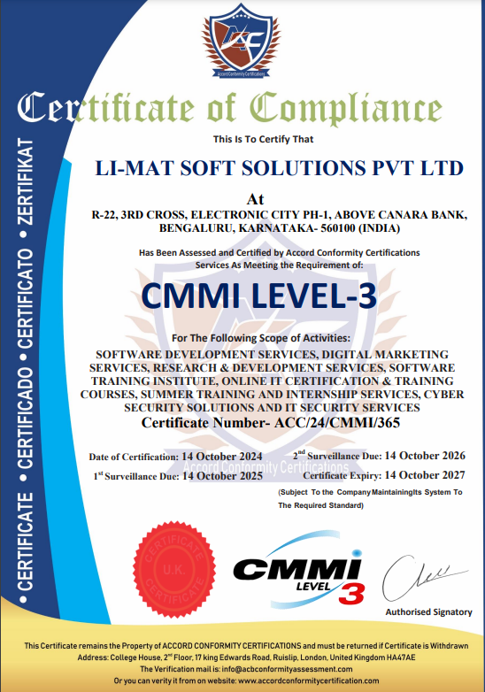
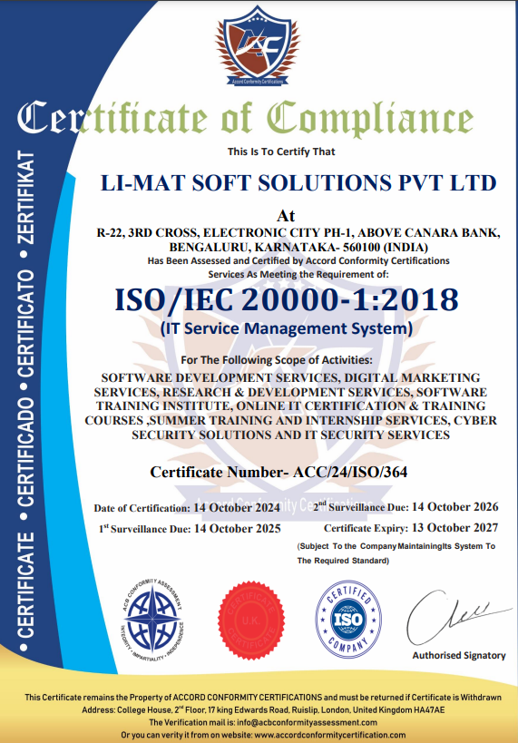
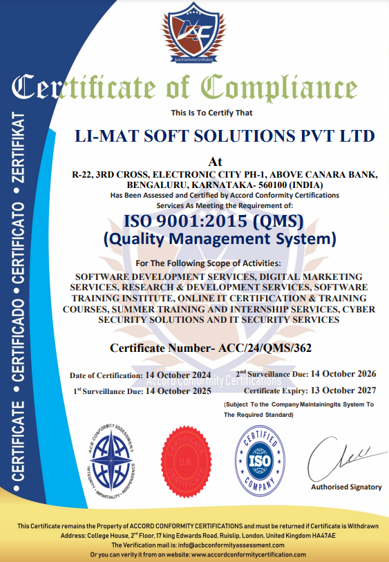
VLSI Internship Certificate

EDA Tools

Hands-on Lab Practice

Learning Format

Design & Simulation Labs

Batch Starts

Monthly Cohorts

Core Tech

Verilog & RTL

Advanced VLSI Program Highlights

Unlock the secrets of semiconductor engineering. Our program bridges the gap between digital logic theory and professional chip design workflows used by industry giants.

Verilog

Verilog HDL Mastery

Learn to model complex digital systems using Verilog for implementation on FPGA and ASIC.

RTL

RTL Design Flow

Master the standard cell-based design flow from specification to netlist generation.

Verification

FPGA Verification

Prototype your designs on live FPGA boards (Xilinx/Altera) and verify real-time performance.

Analog

CMOS Technology

Understand the physics of MOS transistors, logic gates, and VLSI physical design constraints.

EDA

EDA Tool Proficiency

Gain hands-on experience with industry tools like Cadence, Mentor Graphics, or open-source tools.

Static

Static Timing (STA)

Learn critical path analysis, setup/hold time constraints, and timing closure techniques.

VLSI Design Ecosystem

Chip Design Lifecycle

VLSI engineering is what makes your smartphones and computers possible. Our internship covers the front-end design cycle, focusing on RTL coding, functional verification, and logic synthesis. You will learn how high-level specifications are transformed into billions of transistors on a silicon wafer.

VLSI Semiconductor Chip

Domain Specializations

Front-End Design

Architecture definition, RTL coding, and functional bug tracking.

Design Verification

Writing testbenches, assertions, and using UVM/OVM methodologies.

Physical Design

Floorplanning, Placement, Routing, and GDSII generation basics.

Analog VLSI

Designing OP-AMPS, DACs, and high-speed analog-to-digital converters.

VLSI Career Roadmap

A structured 40-day transition from digital logic foundations to professional chip design.

Phase 1

Digital Electronics & Verilog Foundations

Strengthening digital logic concepts and introducing Verilog HDL.

  • Combinational & Sequential Circuits
  • Number Systems & Boolean Logic
  • Introduction to FSM (Finite State Machines)
  • Verilog Basics: Syntax & Structure
  • Behavioral vs Dataflow Modeling
  • Writing Simple Verilog Modules
Phase 2

RTL Design & Simulation

Building and testing RTL modules using simulation tools.

  • RTL Design Concepts
  • Designing Registers, Counters & ALUs
  • Memory Design Basics (Simple RAM/ROM)
  • Writing Testbenches in Verilog
  • Simulation: ModelSim / Vivado Simulator
  • Debugging using Waveforms
Phase 3

FPGA Implementation Basics

Taking designs from simulation to real hardware prototyping.

  • FPGA Architecture Fundamentals
  • Using Xilinx Vivado Toolchain
  • RTL Synthesis Basics
  • Pin Configuration & Constraints
  • Bitstream Generation
  • Uploading Design to FPGA Board
Phase 4

Mini Project & Industry Preparation

Applying RTL design knowledge in a guided industrial project.

  • Designing Digital Systems (Processor Blocks)
  • RTL Optimization Basics
  • Intro to Verification Concepts
  • Debugging on Hardware
  • Resume Building for VLSI Roles
  • Interview Prep & Career Guidance

VLSI Tools & Languages

Verilog HDL SystemVerilog Xilinx Vivado ModelSim Cadence Virtuoso CMOS Logic FPGA (Artix-7) Static Timing Analysis ASIC Flow Tcl Scripting

Why Join VLSI Internship?

High-demand skills for the booming semiconductor industry in India.

Silicon Focus

Work on real-world chip design scenarios rather than just theoretical circuits.

Standard EDA Tools

Gain proficiency in tools used by Intel, Qualcomm, and NVIDIA engineers.

Industrial Mentors

Learn from professionals who have designed taped-out chips at top SOC firms.

FPGA Prototyping

Test your logic real-time on physical hardware to understand timing and power.

Verified Credential

Earn a certificate that validates your RTL design and Verification skills to employers.

Tier-1 Placements

Job support for roles like RTL Designer, DV Engineer, and Synthesis Engineer.

Companies Hiring VLSI Engineers

Intel
Qualcomm
NVIDIA
AMD
ARM
TCS VLSI
Wipro

One Step Closer to a VLSI Career

Unlock the highest-paying engineering roles with our expert-led VLSI program.

VLSI Design & Verification

Rs. 12,000/- Rs. 15,000/-

Limited Seats * 40-Day Industrial Program

  • 40-Days Intensive Industrial Training
  • Full Access to EDA Simulation Tools
  • Verilog HDL & RTL Design Boot Camp
  • FPGA Real-time Prototyping Sessions
  • Internship Certificate + Portfolio Help
  • Mock Interviews for Core Companies
  • 100% Industry Oriented Projects
Secure Your Enrollment
Next Batch Starts March 15, 2026

500+

Logic Designs Verified

4.8/5

Tool Training Satisfaction

$10B+

Chip Industry Growth

BUILD THE FUTURE OF SILICON

Expertise in Chip Design is the ultimate career edge.

Enroll for VLSI Program

Our Compliances

CMMI Level 3 Compliance Certificate
ISO/IEC 20000 Compliance Certificate
ISO/IEC 27001 Compliance Certificate
ISO 9001 Compliance Certificate
Request a Call Back

Our Compliances

Images
Images
Images
Images
Images